I am inspired by opportunities to develop novel quantum computing devices and fabrication and characterization processes that enable unprecedented insights into complex materials science challenges.
▶️ 𝗛𝗢𝗪 𝗜𝗧 𝗕𝗘𝗚𝗔𝗡:
My hands-on problem-solving approach developed from a love for fixing stuff and a need for being self-sufficient. During the war, I learned to repair expensive items, such as cars and appliances, on my own.
I went on to earn a B.Sc., which sparked my interest in semiconductors and novel materials, earned a scholarship from U.N. to pursue an M.Sc. in material science and engineering in South Korea, and later, a Ph.D. in engineering physics.
▶️ 𝗪𝗛𝗔𝗧 𝗜’𝗠 𝗗𝗢𝗜𝗡𝗚:
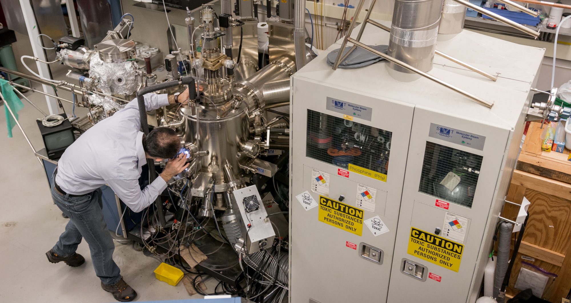
For the last 10 years, I have led and collaborated on complex research projects that explored new materials and novel devices with applications in lasers, detectors, optical modulators, and solar cells. Along the way, I solidified my expertise in III-V compound semiconductor growth, epitaxial system development, and device fabrication processes which supported 50+ publications.
I have also proven myself as a leader, overseeing the daily facility operations, including a major retrofitting and expansion project, and the procurement, installation, commission, and preventative maintenance of $10M+ in equipment.
▶️ 𝗠𝗬 𝗞𝗘𝗬 𝗧𝗥𝗔𝗜𝗧𝗦:
⚙️Root Cause Problem Solving | My sharp eyes and strong attention to detail help me quickly identify and stop issues from propagating and prevent several weeks of lost time and thousands in repairs.
⚙️Ownership & Accountability | I am always looking at the downstream effects and strive to build strong vendors networks to source the right materials and services at the right price to get the job done right (and well).
⚙️Project Management | As a Certified Project Manager, I apply agile and predictive methodologies to drive continuous process and operating improvements and manage and anticipate risks.
⚙️Semiconductor Equipment | MBE, MOCVD, PECVD, LPCVD, ALD, e-beam/thermal evaporation, DC/RF sputtering, ion implantation, SEM, TEM, XRD, RIE, ICP, DRIE, photolithography, MEIS, RBS, EDX, XPS, ToF-SIMS, UV-Vis, FTIR, AFM
▶️ 𝗠𝗬 𝗡𝗘𝗫𝗧 𝗠𝗢𝗩𝗘:
I’m eager to drive advancements in nanotechnology and semiconductors, improve quantum device development, and advance the production of faster and more efficient computers to solve challenging problems.
Connect with me via LinkedIn or contact me.